Understanding the Five Critical Threats and the Minimum Necessary Protection
An educational guide for engineers and procurement professionals in semiconductor and precision electronics
In semiconductor and precision electronics manufacturing, the “last mile” from factory to customer is often the most overlooked stage. Engineers invest enormous effort in product design and process optimization, yet frequently settle for “good enough” shipping packaging. However, industry data shows that transport-related damage accounts for 8%-15% of total defect rates, with ESD damage, moisture ingress, and physical impact being the three leading causes.
This article examines the five critical threats facing precision electronic components during shipping, and explains why industry best practice demands a three-layer protection packaging system.
1. Electrostatic Discharge: The Invisible Threat to Precision Components
Electrostatic Discharge (ESD) is the most pervasive and difficult-to-prevent threat during component shipping. Static charges generated by a person simply walking can reach 3,000-35,000 volts, while most semiconductor devices have ESD withstand thresholds of only 200-2,000 volts. Even more dangerous, discharges below the human perception threshold (~3,500V) can still cause device damage.
ESD damage manifests in two forms:
1. Hard Failure: Immediate functional loss, detectable during outgoing quality inspection.
2. Latent Damage: Device passes testing but has developed microscopic damage pathways that cause field failures weeks or months later. Latent ESD damage is the primary driver of customer complaints and warranty costs.
ESD Protection Levels:
1. Conductive materials (surface resistivity < 10⁴ Ω/sq): Provide rapid charge dissipation pathways — e.g., conductive injection molded boxes.
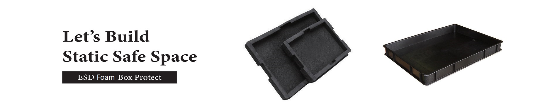
2. Static dissipative materials (surface resistivity 10⁴ - 10¹¹ Ω/sq): Dissipate charges at a controlled rate — e.g., ESD foam.
3. Shielding materials: Block external electric fields — e.g., metallized shielding bags.
Single-layer ESD protection leaves gaps. For example, using only a conductive box without a shielding bag means external electric fields can still penetrate through gaps in the box to affect internal components. Three-layer ESD protection (conductive box + dissipative foam + shielding bag) creates a complete Faraday cage effect for comprehensive electrostatic isolation.
2. Moisture Ingress and the “Popcorn Effect”: The Underestimated Mass Rejection Risk
The IPC/JEDEC J-STD-033 standard classifies electronic components into 8 Moisture Sensitivity Levels (MSL 1 through MSL 6). Higher MSL ratings mean shorter allowable exposure times (Floor Life) after removal from dry packaging.
|
MSL Level |
Floor Life (Exposure Limit) |
Storage Requirements |
|
MSL 1 |
Unlimited |
No special requirements |
|
MSL 2 |
1 year |
≤30°C / 60% RH |
|
MSL 2a |
4 weeks |
≤30°C / 60% RH |
|
MSL 3 |
168 hours (7 days) |
≤30°C / 60% RH |
|
MSL 4 |
72 hours |
≤30°C / 60% RH |
|
MSL 5 |
48 hours |
≤30°C / 60% RH |
|
MSL 5a |
24 hours |
≤30°C / 60% RH |
|
MSL 6 |
Mandatory bake before reflow |
Forced dry storage |
When moisture-sensitive components absorb excessive moisture, the water inside the package rapidly vaporizes and expands during reflow soldering (typically 260°C), generating enormous internal vapor pressure. This causes:
1. Internal delamination
2. Lead frame separation from the mold compound
3. Package cracking — the industry-known “Popcorn Effect”
This failure typically occurs during the customer’s SMT reflow process, meaning entire batches may be scrapped, with the supplier facing significant claims.
Proper moisture-barrier packaging: Place products in a Moisture Barrier Bag (MBB) with desiccant and a Humidity Indicator Card (HIC), then vacuum seal. This maintains internal humidity below safe thresholds, ensuring Floor Life resets from the moment of unsealing.
3. Transport Vibration and Shock: The Life-or-Death Test for 0.4mm Pitch Leads
Modern electronic packages are increasingly fine-pitched:
1. QFP lead pitch can be as low as 0.4mm
2. BGA solder ball diameter is typically 0.3-0.76mm
3. Optical component surface roughness requirements: Ra < 1nm
4. MEMS device mechanical structures at micrometer scale
During transport, products may experience:
1. Random vibration from truck transport (5-200Hz, 0.5-2g RMS)
2. Drop impact (a 1.2m drop can produce hundreds of g’s of instantaneous acceleration)
3. Stacking compression
Without professional cushioning and fixation, components shift and collide during transport, resulting in: lead deformation, solder ball detachment, optical surface scratching, and MEMS microstructure fracture. These are all irreversible damage.
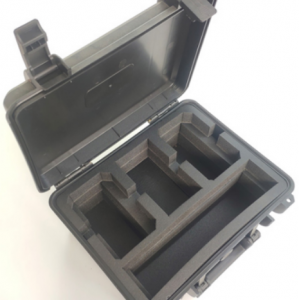
The correct approach is “rigid outside, soft inside”:
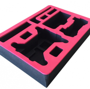
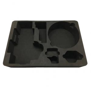
1. Outer rigid shell (injection molded box) resists external compression and impact.
2. Inner flexible liner (custom-cut foam) provides cushioning and precise positioning, ensuring each component sits in its own foam cavity with zero displacement.
4. Electromagnetic Interference and Environmental Contamination: Two Often-Overlooked Dimensions
Electromagnetic Interference (EMI)
During transit, products pass through various electromagnetic environments: wireless equipment in warehouses, vehicle electronic systems, heavy machinery at ports, etc. For EMI-sensitive devices like RF front-end modules and high-speed optical transceivers, external electromagnetic fields can cause:
1. Stored charge redistribution
2. Bit flips in EEPROM/Flash memory
3. Parameter drift in sensitive analog circuits
Metallized shielding bags create an electromagnetic barrier that effectively isolates internal components from external field interference.
Environmental Contamination
The shipping environment is far harsher than a cleanroom:
1. Dust particles settle on solder pads, reducing solderability
2. Salt spray during coastal shipping accelerates metal surface oxidation
3. Industrial SOx, NOx, and other chemical gases react with metal surfaces
Vacuum-sealed shielding bags create a micro-cleanroom environment, completely isolating products from all external contamination sources.
5. Three-Layer Protection: Not Over-Engineering, But Minimum Necessary Protection
Understanding the five threats above, the design logic of three-layer protection becomes clear:
|
Protection Layer |
Core Function |
Threats Addressed |
|
Layer 1: Conductive Injection Molded Box |
Rigid physical protection + near-field ESD dissipation |
Physical impact, near-field ESD |
|
Layer 2: ESD Foam Inserts |
Cushioning + precise fixation + ESD dissipation |
Transport vibration, component displacement, contact ESD |
|
Layer 3: Shielding Bag with Vacuum Seal |
Moisture barrier + EMI shielding + contamination prevention |
Moisture, EMI, environmental pollution |
Each layer addresses an independent set of problems. Removing any single layer creates protection gaps. This is not over-engineering — it is the minimum necessary protection configuration recommended by IPC/JEDEC and other industry standards.
6. Packaging Cost vs. Quality Loss Cost: A Simple Economic Calculation
Some procurement decision-makers may ask: does three-layer packaging add too much cost?
Let’s do the math:
4. A single optical transceiver module typically costs tens to hundreds of dollars
5. A complete three-layer packaging set (molded box + foam + shielding bag) costs only 1%-3% of product value
6. A single batch quality claim due to inadequate packaging — involving returns, rework, reshipping, and customer trust erosion — typically costs 50-100x the packaging cost
Moreover, using standardized universal box models with custom-cut foam avoids the high tooling costs (typically tens of thousands of dollars) and long development cycles (typically 6-8 weeks) of fully custom injection molded trays. This represents the optimal balance of protection performance and economics.
Conclusion
Shipping packaging for precision electronic components is not “the last step in production” — it is a critical link in the product quality assurance chain. Choosing the right packaging solution means protecting your products, protecting your customer relationships, and protecting your brand reputation.
If you are looking for a one-stop ESD packaging solution, read our detailed case study: “One-Stop Shipping Packaging Solution for Precision Electronic Components” to learn how our standardized box + custom foam + shielding bag combination provides comprehensive transport protection for optical modules, MEMS sensors, RF modules, and other high-value components.